Авторитетность издания

Добавить в закладки
Следующий номер на сайте


An optimized design of serial logic comparator
Abstract:Comparator is a combinational circuit which is used to compare the values by taking two numbers as input and determines whether one number is greater than, less than or equal to the other number. Com-parators have many applications in mainstream electronics and modern digital VLSI design, such as – Threshold Detector, Zero crossing Detector, Relaxation Oscillator, Schmitt Trigger and digital signal processors. This paper presents an efficient serial comparator design by block optimization techniques. The proposed 8-bit binary serial comparator is designed using a parallel to serial converter circuit as first stage that converts parallel data into serial rotated data. The second stage involves implement-ing a switching circuit in order to place data in two-comparison shift register. Only Most Significant Bit values of the two registers are compared through one-bit comparator cell as the third stage. The design and simulation of the proposed miniaturized global circuit of the serial comparator has been imple-mented by using DSCH 3.5 and Microwind 2.0 software showing a good quality performance. Moreo-ver, the paper describes the simulation of layout and parametric analysis for the proposed 8-bit com-parator design. It is noted that the area cost, the number of cycles and power consumption values are less in the proposed technique compared to the existing approaches.
Аннотация:В статье рассматривается один из важнейших элементов информационной системы – компаратор. Это комбинационная схема, которая используется для сравнения значений, принимая два числа в качестве входных данных и определяя, каким является каждое из них: больше, меньше или равно другому числу. Компараторы имеют множество применений в основной электронике и в современных цифровых СБИС, таких как пороговый детектор, детектор пересечения нуля, генератор релаксации, триггер Шмитта, процессоры цифровых сигналов. Анализируются основные научные работы о проектировании компаратора. Во многих из них, направленных на минимизацию потерь энергии и площади проектируемого компаратора, подчеркивается актуальность проблемы. Представлена эффективная конструкция 8-разрядного последовательного компаратора, основанная на методах блочной оптимизации. На первом этапе предлагаемый компаратор преобразует параллельные данные в последовательные. На втором этапе реализуется переключение для размещения данных в сдвиговом регистре. Только значения старшего бита двух регистров сравниваются через однобитовую ячейку компаратора в качестве третьего этапа. Предложенные миниатюрные схемы последовательного компаратора были реализованы с использованием программного обеспечения DSCH 3.5 и Microwind 2.0 и продемонстрировали хорошую работу. В статье рассматриваются также моделирование компоновки и параметрический анализ предлагаемой конструкции 8-битного компаратора. Предложенный последовательный компаратор требует меньше площади, количества циклов и потребляемой мощности по сравнению с существующими подходами.
| Авторы: Нийонсаба T. (nitherence5@gmail.com) - Университет Бурунди (преподаватель-исследователь), Бужумбура, Бурунди, Ph.D, Акимана А. (armelblackbox@gmail.com) - Университет Бурунди (инженер), Бужумбура, Бурунди, Кибея Х. (kibeyahassan@gmail.com) - Университет Бурунди (преподаватель-исследователь), Бужумбура, Бурунди, Ph.D, Увизейимана П. (uwizeyimanaprovi@gmail.com) - Университет озера Танганьика Бужумбура (магистр, доцент), Кигобе, Бурунди | |
| Keywords: optimized comparator, miniaturized circuit, switching circuit, converter, logic comparator |
|
| Ключевые слова: оптимизированный компаратор, миниатюризованная схема, переключающая схема, конвертер, логический компаратор |
|
| Количество просмотров: 1806 |
Статья в формате PDF |
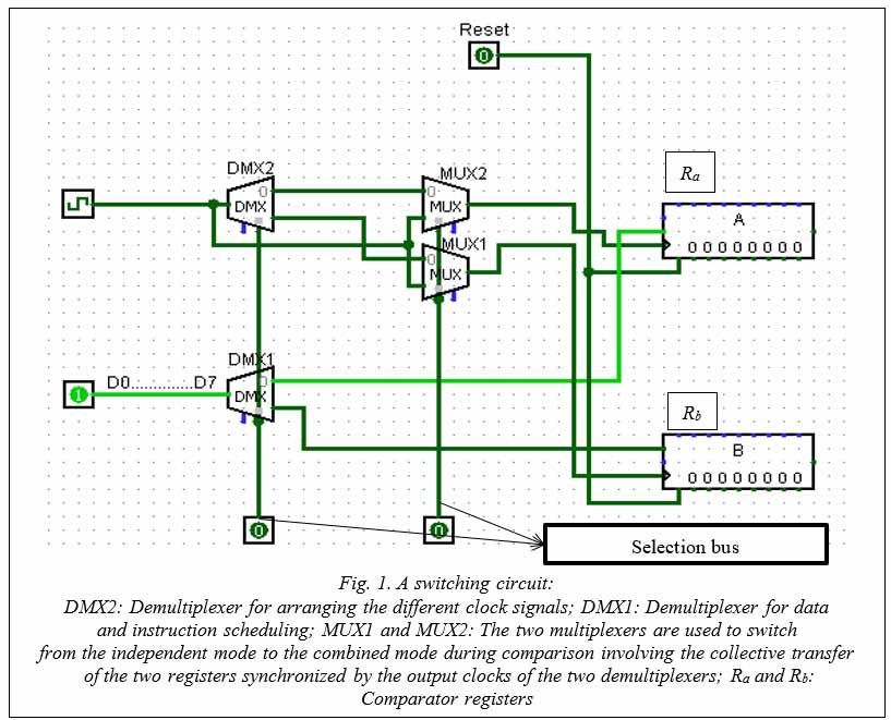
The increasing complexity of digital circuits requires constant improvement of design methods and tools. In many papers, comparator’s designing use one and two bit [1]. Some works propose the design and optimization of n-bit reversible binary comparator [2]. Several improvements have been made to digital circuits to minimize the effect of modulating the length of the channel, to stabilize the control voltage against varying the power supply of the digital circuits, converter of the signal from parallel to series [3]. The binary comparators are designed using a circuit for the most significant bit at the first stage to compare MSBs and a one-bit comparator cell at the second stage and so on to compare a lesser significant bit position. The comparators like 74LS85, 7485, and others compare two bits of two numbers, starting with the most significant bit. This operation involves several logic gates, which are the source of the system complexity and greediness. There are several researches aimed at minimizing energy loss by using circuits built from n Reversible Logic Gates [2, 4, 5], and Quantum-Dot Cellular Automata [6], but the problem of circuit miniaturization and energy saving remains rele- vant. The area and power of the Designed Compar- ator is also a topical issue. There are some re- searches in that area such as comparator Design us- ing Hybridized Full Adder Module based on PTL and GDI Logic and 4 Bit Comparator Design Based on Reversible Logic Gates [7, 8]. The Circuit arrangement converting parallel data into serial data is the subject of an innovation patent application [9, 10]. This circuit is not minimized and therefore remains energy intensive. Several researches are aimed at miniaturizing digital circuits in order to overcome the above-mentioned problems. Despite the multitude of research work to resolve the mentioned problem, it is still relevant today. Our research work contributes to solving the problem of digital circuit miniaturization. We are bringing a building block to solve this problem by designing a miniaturized serial digital comparator that is less complex and therefore less energy intensive. The paper is organized into the following sections. First of all, section 2 describes a parallel to serial converter. Then, section 3 represents a switching circuit. A new design of miniaturized global circuit of the serial comparator and result analysis of the proposed design is presented respectively in section 4 and 5. Finally, there is a conclusion. The input data of the system are usually parallel since they come from the memories and the various sensors. These data must be serially converted to enter the comparator registers. The conversion circuit is a multiplexer automatically selected by a binary counter, which allows reading the bits one by one. The data will then be routed to a specific register by decoding address (i.e. a single output activated among several). A miniaturized conversion circuit is shown in Figure (http://www.swsys. ru/uploaded/image/2022-2/2022-2-dop/11.jpg).
The converted data must be transferred to the shift registers that are specifically addressed. The data transfer must be synchronized by a clock that sends a bit at each clock pulse. The switching process is performed by two demultiplexers who have the same size (the same number of outputs) selected by the same address. The serial comparison consists to compare two values in binary in a serial way. First, it is necessary to carry out a rotation of these values in the following way: Normally the data is arranged like this at the input of the parallel to serial converter circuit D = D7 … D0. During conversion, the data are rotated and enter the right shift registers of comparator. In the registers, the data are as fol- lows: a = a0 ... a7. With a0 the Most Significant Bit (MSB) and a7 the Least Significant Bit (LSB), b = b0 … b7. Where, a, b – numbers, R – register, Ra and Rb – register of a and b respectively, n – nth bit of a or b. The truth table of 1-bit Comparator of the classic comparison is shown in Table. The truth table of 1-bit Comparator of the classic comparison
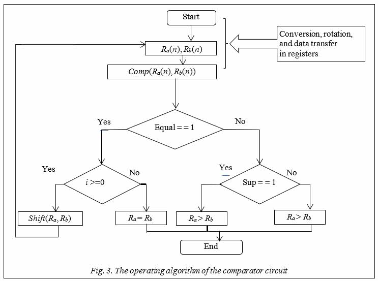
The comparator compares two bits with the same weight. For example: Ra (7) will be compared to Rb (7). If two bits are equal, we have: F(Xn): Ra(n) = Rb(n). Then we continue comparison till the end. If all bits with the same weight are equals, we retain the equality. Else if an inequality is detected, the decision of inequality is made and the process of comparison is stopped. The inequality detection circuit triggers immediately stop. So the time allocated to the comparison must be equal to the number of bits in the registers, i.e. if the registers are 8 bits long, 8 cycles will be necessary at maximum. 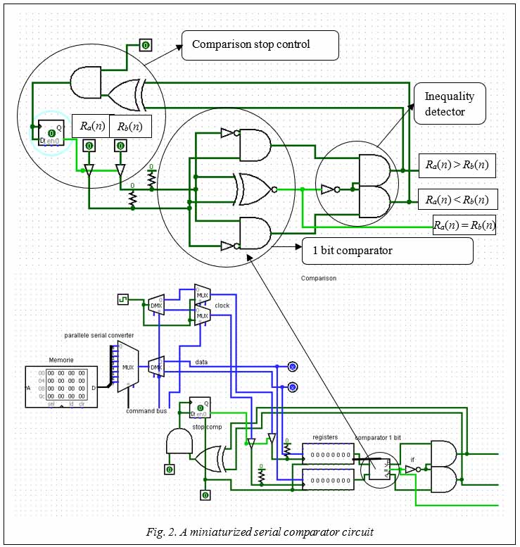 Two figures (http://www.swsys.ru/uploaded/ image/2022-2/2022-2-dop/11.jpg, Fig. 2) show serial data that can enter the comparator in a synchronized way. The switching circuit sends the data to the two comparator registers. The latter can make a bit by bit comparison. The global circuit shown in Figure 2 includes the parallel-serial converter, which converts the data from memories, sensors into serial data while also performing a rotation. These data are directed towards the registers of the comparator by a switching circuit. At every clock pulse both registers perform a right shift of the serial data. The shift is synchronized by a clock. The miniaturized global circuit of the serial comparator is shown in Figure 2. The simulation was done in the software Logisim 2.7.0. The comparator operation principle is to compare two bits Ra(n) and Rb(n) that come out of two shift registers. At each shift, a bit of the register Ra and Rb are shifted to the right. The right shift oper- ation must be synchronous. The comparison logic consists in comparing the first MSB (most significant bit) of Ra and Rb. If an inequality is encountered, the comparison stops and the decision is made. In order for the most significant bits to be the first to be compared, the binary representation of the numbers to be compared must be inverted (rotation). A 1-bit comparator is enough to compare two numbers of any size. The detector allows finding out the inequality of bits when the inequality is detected, a logic gate xor switches to the high state; this change of state activates a monostable that disables the clock input buffers of both registers Ra and Rb and the shift right operation stops. Therefore, the comparison stops as well. The advantage of this comparator is that the register width does not influence the comparator structure since it compares only two bits, which considerably reduces the number of logic gates used. The data input of the shift registers are serial, so the width of the data bus is significantly reduced. The global circuit of the serial comparator starts by converting the parallel data into serial data by performing a rotation, as many pulses as there are bits. Then, if data are represented in series, the comparison should be carried out. The comparison is done as usual. If the bits of the same rank are equal, a right shift will be done. Figure 3 shows the operating algorithm of the comparator circuit. Result analysis
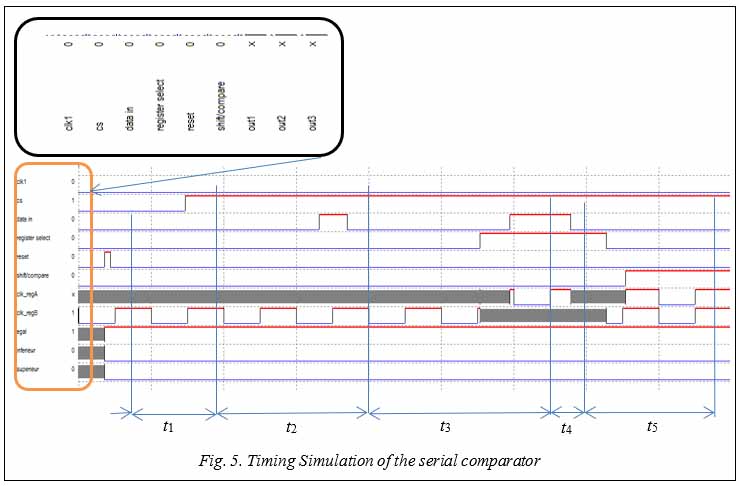
Timing Simulation. It is necessary to validate the schematic of logic circuit. To overcome this problem DSCH and MICROWIND 2.0 designing tools works simultaneously. First, the design is simulated in DSCH designing tools to know the exact functionality of the circuit and then implemented on the layout in microwind. Figure 5 shows timing simulation of the proposed serial comparator. With: t1 : reset, t2 : activation of the comparison, t3 : data transmission in A, t4 : data transmission in B, t5: comparison. Figure 5 shows the operation of the global comparison circuit at time t1, the circuit is reset to zero by a pulse on reset.
Layout analysis. The layout designing has been automatically generated. The verilog file has been generated by the DSCH 3.5 tool which is compiled by the MICROWIND 2.0. This Figure shows the layout of a designing circuit (http://www.swsys.ru/ uploaded/image/2022-2/2022-2-dop/12.jpg). The layout size is the following: width 627.5 μm (1255 lambda), height 148.0 μm (296 lambda), surf 92870.0 μm2 (0.1 mm2). The designed circuit of the serial comparator has been simulated using DSCH 3.5 and Microwind 2.0. The results and others parameters are shown in the Figures (http://www.swsys.ru/ uploaded/image/2022-2/2022-2-dop/13.jpg). Conclusion The authors have proposed a miniaturized efficient 8-bit comparator design by using block optimization approach. The proposed 8-bit comparator circuit can work efficiently with minimum complexity. It is evident from the simulation results that the comparator circuit has been successfully executed and simulated on DSCH 3.5 tool, which is compiled by the MICROWIND 2.0. Hence this design can be used in implementation of n-bit and can be used in various applications. References 1. Singh A., Kumar S., Manhas P. Implementation of comparator using different styles of modeling. Proc. Int. Conf. on Latest Trends in Electronics & Communication Engineering, Greater Noida, 2019. 2. Aggarwal M., Mehra R. Performance analysis of magnitude comparator using different design techniques. Int. J. of Computer Applications, 2015, vol. 115, no. 14, pp. 12–15. DOI: 10.5120/20218-2496. 3. Sokol M., Galajda P., Pecovsky M. Improving Input Circuits for 7-bit Flash AD Converter. Proc. XXX Int. Conf. Radioelektronika, 2020, pp. 1–5. DOI: 10.1109/RADIOELEKTRONIKA49387.2020.9092400. 4. Jayashree H.V., Agarwal V.K., Charan P.V., Kariappa A.M.C. Design of fault tolerant n bit reversible comparator for optimization of garbage and Ancilla bits. Proc. of Int. Conf. on Circuits, Communication, Control and Computing, 2014, pp. 21–24. DOI: 10.1109/CIMCA.2014.7057748. 5. Sharma A., Sharma P. Area and power efficient 4-bit comparator design by using 1-bit full adder module. Proc. Int. Conf. on Parallel, Distributed and Grid Computing, 2014, pp. 1–6. DOI: 10.1109/PDGC. 2014.7030705. 6. Vaghela R.S., Ghandhi P.P. Design and analysis of low offset high speed dynamic comparator. IJMTER, 2016, vol. 3, no. 5, pp. 1–7. 7. Latha B.C., Kumar V.P., Tech M. Design of reversible comparators with priority encoding using Verilog HDL. IJLEMR, 2016, no. 7. Available at: http://www.ijmetmr.com/oljuly2016/BChaitanyaLatha-VPraveenKumar-25.pdf (accessed February 12, 2022). 8. Svendsen G.D. Convertisseur de Données Parallèle – Série Synchrone a Rapport de Fréquence Programmable. Demande de Brevet d’Invention, no. 83 03434. 9. Razavi B. The StrongARM Latch [a circuit for all seasons]. IEEE Solid State Circuits Magazine, 2015, vol. 7, no. 2, pp. 12–17. DOI: 10.1109/MSSC.2015.2418155. 10. Snehalatha G., Akhila M., Snehalatha G. Design and implementation of low power VCO based ADC using TIQ comparator in cadence using 45nm Technology. IJMTER, 2017, vol. 4, no. 8, pp. 191–201. DOI: 10.21884/IJMTER.2017.4269.K2BG5. Литература 1. Singh A., Kumar S., Manhas P. Implementation of comparator using different styles of modeling. Proc. Int. Conf. on Latest Trends in Electronics & Communication Engineering, Greater Noida, 2019. 2. Aggarwal M., Mehra R. Performance analysis of magnitude comparator using different design techniques. Int. J. of Computer Applications, 2015, vol. 115, no. 14, pp. 12–15. DOI: 10.5120/20218-2496. 3. Sokol M., Galajda P., Pecovsky M. Improving Input Circuits for 7-bit Flash AD Converter. Proc. XXX Int. Conf. Radioelektronika, 2020, pp. 1–5. DOI: 10.1109/RADIOELEKTRONIKA49387.2020.9092400. 4. Jayashree H.V., Agarwal V.K., Charan P.V., Kariappa A.M.C. Design of fault tolerant n bit re-versible comparator for optimization of garbage and Ancilla bits. Proc. of Int. Conf. on Circuits, Com-munication, Control and Computing, 2014, pp. 21–24. DOI: 10.1109/CIMCA.2014.7057748. 5. Sharma A., Sharma P. Area and power efficient 4-bit comparator design by using 1-bit full adder module. Proc. Int. Conf. on Parallel, Distributed and Grid Computing, 2014, pp. 1–6. DOI: 10.1109/PDGC. 2014.7030705. 6. Vaghela R.S., Ghandhi P.P. Design and analysis of low offset high speed dynamic comparator. IJMTER, 2016, vol. 3, no. 5, pp. 1–7. 7. Latha B.C., Kumar V.P., Tech M. Design of reversible comparators with priority encoding using Verilog HDL. IJLEMR, 2016, no. 7. URL: http://www.ijmetmr.com/oljuly2016/BChaitanyaLatha-VPraveenKumar-25.pdf (дата обращения: 12.02.2022). 8. Svendsen G.D. Convertisseur de Données Parallèle – Série Synchrone a Rapport de Fréquence Programmable. Demande de Brevet d’Invention, no. 83 03434. 9. Razavi B. The StrongARM Latch [a circuit for all seasons]. IEEE Solid State Circuits Magazine, 2015, vol. 7, no. 2, pp. 12–17. DOI: 10.1109/MSSC.2015.2418155. 10. Snehalatha G., Akhila M., Snehalatha G. Design and implementation of low power VCO based ADC using TIQ comparator in cadence using 45nm Technology. IJMTER, 2017, vol. 4, no. 8, pp. 191–201. DOI: 10.21884/IJMTER.2017.4269.K2BG5. | ||||||||||||||||||||||||||||||

| Постоянный адрес статьи: http://swsys.ru/index.php?page=article&id=4891 |
Версия для печати |
| Статья опубликована в выпуске журнала № 2 за 2022 год. [ на стр. 153-159 ] |
Назад, к списку статей